UltraSPARC II
|
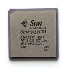
Sun UltraSPARC-II front | |
| Produced | From 1997 to 2004 |
|---|---|
| Designed by | Sun Microsystems |
| Max. CPU clock rate | 250 MHz to 650 MHz |
| Instruction set | SPARC V9 |
| Cores | 1 |
| Predecessor | UltraSPARC |
| Successor | UltraSPARC III |

The UltraSPARC II, code-named "Blackbird", is a microprocessor implementation of the SPARC V9 instruction set architecture (ISA) developed by Sun Microsystems. Marc Tremblay was the chief architect. Introduced in 1997, it was further development of the UltraSPARC operating at higher clock frequencies of 250 MHz, eventually reaching 650 MHz.
The die contained 5.4 million transistors and had an area of 149 mm². It was fabricated by Texas Instruments in their 0.35 µm process, dissipated 25 W at 205 MHz, and used a 2.5 V power supply. L2 cache capacity was 1 to 4 MB.
In 1999, the UltraSPARC II was ported to a 0.25 µm process. This version was code-named "Sapphire-Black". It operated at 360 to 480 MHz, possessed a die area of 126 mm², dissipated 21 W at 400 MHz and the power supply voltage was reduced to 1.9 V. Supported L2 cache capacity was increased to 1 to 8 MB.
Derivatives
The UltraSPARC II was the basis for four derivatives.
UltraSPARC IIe

The UltraSPARC IIe "Hummingbird" was an embedded version introduced in 2000 that operated at 400 to 500 MHz, fabricated in a 0.18 µm process with aluminium interconnects. It dissipated a maximum of 13 W at 500 MHz, used a 1.5 to 1.7 V power supply and had a 256 KB L2 cache.[1]
UltraSPARC IIi
The UltraSPARC IIi "Sabre" was a low-cost version introduced in 1997 that operated at 270 to 360 MHz. It was fabricated in a 0.35 µm process and possessed a die size of 156 mm². It dissipated 21 W and used a 1.9 V power supply. It had a 256 KB to 2 MB L2 cache. In 1998, a version code-named Sapphire-Red, was fabricated in a 0.25 µm process, enabling the microprocessor to operate at 333 to 480 MHz. It dissipated 21 W at 440 MHz and used a 1.9 V power supply.
UltraSPARC IIe+
The UltraSPARC IIe+ or IIi was introduced in 2002. Code-named "Phantom", it operated at 550 to 650 MHz and was fabricated in a 0.18 µm process with copper interconnect. It dissipated 17.6 W and used a 1.7 V power supply. It had a 512 KB L2 cache.
Gemini

The Gemini was the first attempt by Sun to produce a multithreaded microprocessor. It had taped out, but was cancelled before it was introduced after the announcement of UltraSPARC T1 Niagara microprocessor in early 2004. It consisted of two UltraSPARC II cores and an on-die L2 cache on a single chip.
The DAC 2004 abstracts described the dual-core UltraSPARC II processor in Session 40.[2] The "Dual-Core UltraSPARC (2003)" was based upon the UltraSPARC II microarchitecture and featured: DDR-1 memory controller, JBUS interface, parity protected L1 cache, ECC protected dual 512KB on-chip Level 2 cache, 1.2 GHz clock frequency, 80 million transistors, 206mm^2 die size, and dissipated 23 watts of power.[3]
References
- ↑ Levy, Markus (2000-10-12). "Sun may not shine on UltraSparc IIe". EDN. Retrieved 2011-02-16.
- ↑ "SPECIAL SESSION 40: ISSCC Highlights". Sun Microsystems. 2003. Retrieved 2011-02-16.
- ↑ "A Dual-Core 64b UltraSPARC Microprocessor for Dense Server Applications" (PDF). Sun Microsystems. 2003. Retrieved 2011-02-16.
- Kapil, Sanjiv; McGhan, Harlan; Lawrendra, Jesse (2004). "A Chip Multithreaded Processor For Network-Facing Workloads". IEEE Micro. pp. 20–30.