JFET
|
Electric current from source to drain in a p-channel JFET is restricted when a voltage is applied to the gate. | |
| Type | Active |
|---|---|
| Pin configuration | drain, gate, source |
| Electronic symbol | |
  | |

The junction gate field-effect transistor (JFET or JUGFET) is the simplest type of field-effect transistor. They are three-terminal semiconductor devices that can be used as electronically-controlled switches, amplifiers, or voltage-controlled resistors.
Unlike bipolar transistors, JFETs are exclusively voltage-controlled in that they do not need a biasing current. Electric charge flows through a semiconducting channel between source and drain terminals. By applying a reverse bias voltage to a gate terminal, the channel is "pinched", so that the electric current is impeded or switched off completely. A JFET is usually on when there is no potential difference between its gate and source terminals. If a potential difference of the proper polarity is applied between its gate and source terminals, the JFET will be more resistive to current flow, which means less current would flow in the channel between the source and drain terminals. Thus, JFETs are sometimes referred to as depletion-mode devices.
JFETs can have an n-type or p-type channel. In the n-type, if the voltage applied to the gate is less than that applied to the source, the current will be reduced (similarly in the p-type, if the voltage applied to the gate is greater than that applied to the source). A JFET has a large input impedance (sometimes on the order of 1010 ohms), which means that it has a negligible effect on external components or circuits connected to its gate.
History
A succession of FET-like devices were patented by Julius Lilienfeld in the 1920s and 1930s.However, materials science and fabrication technology would require decades of advances before FETs could actually be made. In 1947, researchers John Bardeen, Walter Houser Brattain, and William Shockley failed in their repeated attempts to make a FET. They discovered the point-contact transistor in the course of trying to diagnose the reasons for their failures. The first practical JFETs were made a decade later.
Structure
The JFET is a long channel of semiconductor material, doped to contain an abundance of positive charge carriers or holes (p-type), or of negative carriers or electrons (n-type). Ohmic contacts at each end form the source (S) and the drain (D). A pn-junction is formed on one or both sides of the channel, or surrounding it, using a region with doping opposite to that of the channel, and biased using an ohmic gate contact (G).
Function
JFET operation can be compared to that of a garden hose. The flow of water through a hose can be controlled by squeezing it to reduce the cross section and the flow of electric charge through a JFET is controlled by constricting the current-carrying channel. The current also depends on the electric field between source and drain (analogous to the difference in pressure on either end of the hose).
Constriction of the conducting channel is accomplished using the field effect: a voltage between the gate and the source is applied to reverse bias the gate-source pn-junction, thereby widening the depletion layer of this junction (see top figure), encroaching upon the conducting channel and restricting its cross-sectional area. The depletion layer is so-called because it is depleted of mobile carriers and so is electrically non-conducting for practical purposes.[1]
When the depletion layer spans the width of the conduction channel, pinch-off is achieved and drain-to-source conduction stops. Pinch-off occurs at a particular reverse bias (VGS) of the gate-source junction. The pinch-off voltage (Vp) varies considerably, even among devices of the same type. For example, VGS(off) for the Temic J202 device varies from −0.8 V to −4 V.[2] Typical values vary from −0.3 V to −10 V.
To switch off an n-channel device requires a negative gate-source voltage (VGS). Conversely, to switch off a p-channel device requires positive VGS.
In normal operation, the electric field developed by the gate blocks source-drain conduction to some extent.
Some JFET devices are symmetrical with respect to the source and drain.
Schematic symbols
The JFET gate is sometimes drawn in the middle of the channel (instead of at the drain or source electrode as in these examples). This symmetry suggests that "drain" and "source" are interchangeable, so the symbol should be used only for those JFETs where they are indeed interchangeable.
Officially, the style of the symbol should show the component inside a circle (representing the envelope of a discrete device). This is true in both the US and Europe. The symbol is usually drawn without the circle when drawing schematics of integrated circuits. More recently, the symbol is often drawn without its circle even for discrete devices.
In every case the arrow head shows the polarity of the P-N junction formed between the channel and the gate. As with an ordinary diode, the arrow points from P to N, the direction of conventional current when forward-biased. An English mnemonic is that the arrow of an N-channel device "points in".
Comparison with other transistors
At room temperature, JFET gate current (the reverse leakage of the gate-to-channel junction) is comparable to that of a MOSFET (which has insulating oxide between gate and channel), but much less than the base current of a bipolar junction transistor. The JFET has higher gain (transconductance) than the MOSFET, as well as lower flicker noise, and is therefore used in some low-noise, high input-impedance op-amps.
Mathematical model
The current in N-JFET due to a small voltage VDS (that is, in the linear ohmic region) is given by treating the channel as a rectangular bar of material of electrical conductivity :[3]


where
- ID = drain–source current
- b = channel thickness for a given gate voltage
- W = channel width
- L = channel length
- q = electron charge = 1.6 x 10⁻¹⁹ C
- μn = electron mobility
- Nd = n-type doping (donor) concentration.
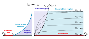
Linear region
Then the drain current in the linear region can be expressed as:

In terms of , the drain current can also be:


Saturation region
The drain current in the saturation region is often approximated in terms of gate bias as:[3]

where
- IDSS is the saturation current at zero gate–source voltage, i.e. the maximum current which can flow through the FET from drain to source at any (permissible) drain-to-source voltage (see, e. g., the I-V characteristics diagram above).
In the saturation region, the JFET drain current is most significantly affected by the gate–source voltage and barely affected by the drain–source voltage.
If the channel doping is uniform, such that the depletion region thickness will grow in proportion to the square root of the absolute value of the gate–source voltage, then the channel thickness b can be expressed in terms of the zero-bias channel thickness a as:

where
- VP is the pinch-off voltage, the gate–source voltage at which the channel thickness goes to zero
- a is the channel thickness at zero gate–source voltage.
See also
References
- ↑ For a discussion of JFET structure and operation, see for example D. Chattopadhyay (2006). "§13.2 Junction field-effect transistor (JFET)". Electronics (fundamentals and applications). New Age International. pp. 269 ff. ISBN 8122417809.
- ↑ J201 data sheet
- 1 2 Balbir Kumar and Shail B. Jain (2013). Electronic Devices and Circuits. PHI Learning Pvt. Ltd. pp. 342–345. ISBN 9788120348448.
External links
| Bipolar junction transistor: | .svg.png) | |
|---|---|---|---|
| Field-effect transistor: | |||
| Multiple transistors: | |||