Deep reactive-ion etching
Deep reactive-ion etching (DRIE) is a highly anisotropic etch process used to create deep penetration, steep-sided holes and trenches in wafers/substrates, typically with high aspect ratios . It was developed for microelectromechanical systems (MEMS), which require these features, but is also used to excavate trenches for high-density capacitors for DRAM and more recently for creating through silicon vias (TSVs) in advanced 3D wafer level packaging technology .
There are two main technologies for high-rate DRIE: cryogenic and Bosch, although the Bosch process is the only recognised production technique. Both Bosch and cryo processes can fabricate 90° (truly vertical) walls, but often the walls are slightly tapered, e.g. 88° ("reentrant") or 92° ("retrograde").
Another mechanism is sidewall passivation: SiOxFy functional groups (which originate from sulphur hexafluoride and oxygen etch gases) condense on the sidewalls, and protect them from lateral etching. As a combination of these processes deep vertical structures can be made.
Cryogenic process
In cryogenic-DRIE, the wafer is chilled to −110 °C (163 K). The low temperature slows down the chemical reaction that produces isotropic etching. However, ions continue to bombard upward-facing surfaces and etch them away. This process produces trenches with highly vertical sidewalls. The primary issues with cryo-DRIE is that the standard masks on substrates crack under the extreme cold, plus etch by-products have a tendency of depositing on the nearest cold surface, i.e. the substrate or electrode.
Bosch process
The Bosch process, named after the German company Robert Bosch GmbH which patented the process,[1][2][3] also known as pulsed or time-multiplexed etching, alternates repeatedly between two modes to achieve nearly vertical structures.
- A standard, nearly isotropic plasma etch. The plasma contains some ions, which attack the wafer from a nearly vertical direction. Sulfur hexafluoride [SF6] is often used for silicon.
- Deposition of a chemically inert passivation layer. (For instance, C4F8 (Octafluorocyclobutane) source gas yields a substance similar to Teflon.)

Each phase lasts for several seconds. The passivation layer protects the entire substrate from further chemical attack and prevents further etching. However, during the etching phase, the directional ions that bombard the substrate attack the passivation layer at the bottom of the trench (but not along the sides). They collide with it and sputter it off, exposing the substrate to the chemical etchant.
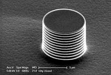
These etch/deposit steps are repeated many times over resulting in a large number of very small isotropic etch steps taking place only at the bottom of the etched pits. To etch through a 0.5 mm silicon wafer, for example, 100–1000 etch/deposit steps are needed. The two-phase process causes the sidewalls to undulate with an amplitude of about 100–500 nm. The cycle time can be adjusted: short cycles yield smoother walls, and long cycles yield a higher etch rate.
Applications
RIE "deepness" depends on application:
- in DRAM memory circuits, capacitor trenches may be 10–20 µm deep,
- in MEMS, DRIE is used for anything from a few micrometers to 0.5 mm.
What distinguishes DRIE from RIE is etch depth: Practical etch depths for RIE (as used in IC manufacturing) would be limited to around 10 µm at a rate up to 1 µm/min, while DRIE can etch features much greater, up to 600 µm or more with rates up to 20 µm/min or more in some applications.
DRIE of glass requires high plasma power, which makes it difficult to find suitable mask materials for truly deep etching. Polysilicon and nickel are used for 10–50 µm etched depths. In DRIE of polymers, Bosch process with alternating steps of SF6 etching and C4F8 passivation take place. Metal masks can be used, however they are expensive to use since several additional photo and deposition steps are always required. Metal masks are not necessary however on various substrates (Si [up to 800 µm], InP [up to 40 µm] or glass [up to 12 µm]) if using chemically amplified negative resists.
Gallium ion implantion can be used as etch mask in cryo-DRIE. Combined nanofabrication process of focused ion beam and cryo-DRIE was first reported by N Chekurov et al in their article "The fabrication of silicon nanostructures by local gallium implantation and cryogenic deep reactive ion etching" (Nanotechnology, 2009).
Precision Machinery
DRIE has enabled the use of silicon mechanical components in high-end wristwatches. According to an engineer at Cartier, “There is no limit to geometric shapes with DRIE,”.[4] With DRIE it is possible to obtain an aspect ratio of 30 or more,[5] meaning that a surface can be etched with a vertical-walled trench 30 times deeper than its width.
This has allowed for silicon components to be substituted for some parts which are usually made of steel, such as the hairspring. Silicon is lighter and harder than steel, which carries benefits but makes the manufacturing process more challenging.
References
- ↑ Basic Bosch process patent application
- ↑ Improved Bosch process patent application
- ↑ Bosch process "Parameter Ramping" patent application
- ↑ Kolesnikov-Jessop, Sonia (23 November 2012). "Precise Future of Silicon Parts Still Being Debated". The New York Times. New York.
- ↑ Yeom, Junghoon; Wu, Yan; Selby, John C.; Shannon, Mark A. (31 October 2005). "Maximum achievable aspect ratio in deep reactive ion etching of silicon due to aspect ratio dependent transport and the microloading effect". J. Vac. Sci. Technol. B.
See also
| Divisions and subsidiaries |
|  | ||||||
|---|---|---|---|---|---|---|---|---|
| Joint ventures and shareholdings |
| |||||||
| Products | ||||||||
| People | ||||||||
| Places | ||||||||
| Other | ||||||||
¹Now integrated into other Bosch divisions or business groupings ²Sold
| ||||||||