AMD 10h
| Produced | From 2007 to 2012 |
|---|---|
| Common manufacturer(s) | |
| Max. CPU clock rate | 1700 MHz to 3700 MHz |
| FSB speeds | 1000 MHz to 2000 MHz |
| Min. feature size | 65 nm to 45 nm |
| Instruction set | AMD64 (x86-64) |
| Socket(s) | |
| Predecessor | K8 - Hammer |
| Successor | Bulldozer - Family 15h |
| Core name(s) |
The AMD Family 10h, or K10, is a microprocessor microarchitecture by AMD based on the K8 microarchitecture.[1] Though there were once reports that the K10 had been canceled,[2] the first third-generation Opteron products for servers were launched on September 10, 2007, with the Phenom processors for desktops following and launching on November 11, 2007 as the immediate successors to the K8 series of processors (Athlon 64, Opteron, 64-bit Sempron).
Nomenclatures
It is commonly perceived by the PC community that from the time after the use of the codename K8 for the AMD K8 or Athlon 64 processor family, AMD no longer uses K-nomenclatures (originally stood for Kryptonite[3]) since no K-nomenclature naming convention beyond K8 has appeared in official AMD documents and press releases after the beginning of 2005.
The name "K8L" was first coined by Charlie Demerjian, one of the writers of The Inquirer back in 2005,[4] and was used by the wider IT community as a convenient shorthand [5] while according to AMD official documents, the processor family was termed "AMD Next Generation Processor Technology".[6]
The microarchitecture has also been referred to as Stars, as the codenames for desktop line of processors was named under stars or constellations (the initial Phenom models being codenamed Agena and Toliman).
In a video interview,[7] Giuseppe Amato confirmed that the codename is K10.
It was revealed, by The Inquirer itself, that the codename "K8L" referred to a low-power version of the K8 family, later named Turion 64, and that K10 was the official codename for the microarchitecture.[5]
AMD refers to it as Family 10h Processors, as it is the successor of the Family 0Fh Processors (codename K8). 10h and 0Fh refer to the main result of the CPUID x86 processor instruction. In hexadecimal numbering, 0Fh (h represents hexadecimal numbering) equals the decimal number 15, and 10h equals decimal 16. (The "K10h" form that sometimes pops up is an improper hybrid of the "K" code and Family identifier number.)
Schedule of launch and delivery
Timeline
Historical information
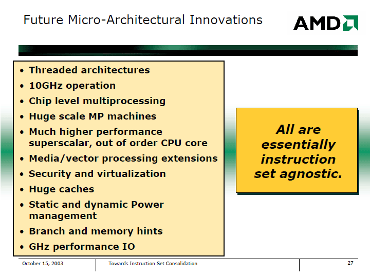
In 2003, AMD outlined the features for upcoming generations of microprocessors after the K8 family of processors in various events and analyst meetings, including the Microprocessor Forum 2003.[8] The outlined features to be deployed by the next-generation microprocessors are as follows:
- Threaded architectures.
- Chip level multiprocessing.
- Huge scale MP (multi-processor) machines.
- 10 GHz operation.
- Much higher performance superscalar, out of order CPU core.
- Huge caches.
- Media/vector processing extensions.
- Branch and memory hints.
- Security and virtualization.
- Enhanced Branch Predictors.
- Static and dynamic power management.
On April 13, 2006, Henri Richard, AMD executive vice president and chief officer for marketing and sales, acknowledged[9] the existence of the new microarchitecture in an interview.
In June 2006, AMD executive vice president Henri Richard had another interview with DigiTimes commented on the upcoming processor developments:
Q: What is your broad perspective on the development of AMD processor technology over the next three to four years?A: Well, as Dirk Meyer commented at our analysts meeting, we're not standing still. We've talked about the refresh of the current K8 architecture that will come in '07, with significant improvements in many different areas of the processor, including integer performance, floating point performance, memory bandwidth, interconnections and so on.
— AMD Executive Vice President, Henri Richard, Source: DigiTimes Interview with Henri Richard[10]
Confirmation of time frames

On July 21, 2006, AMD President and Chief operating officer (COO) Dirk Meyer and Senior VP Marty Seyer confirmed that the launch date of new microprocessors of Revision H under the new microarchitecture is slated for the middle of 2007; and that it will contain a quad core version for servers, workstations, and high-end desktops, as well as a dual core version for consumer Desktops. Some of the Revision H Opterons shipped in 2007 will have a thermal design power of 68 W.
On August 15, 2006, at the launch of the first Socket F dual-core Opterons, AMD announced that the firm had reached the final design stage (tape-out) of quad-core Opteron parts. The next stages are testing and validation, with sampling to follow after several months.[11]
On June 29, 2007, AMD stated that server processors codenamed Barcelona will ship in August 2007, and corresponding server systems from partners will ship in September of the same year.[12]
On August 13, the reported ship dates for the first Barcelona processors were set for September 10, 2007. They announced the Opteron 2348 and 2350 will have core frequencies of 1.9 GHz and 2.0 GHz.[13]
TLB Bug
In November 2007 AMD stopped delivery of Barcelona processors after a bug in the translation lookaside buffer (TLB) of stepping B2 was discovered that could rarely lead to a race condition and thus a system lockup.[14] A patch in BIOS or software worked around the bug by disabling cache for page tables, but it was connected to a 5 to 20% performance penalty. Kernel patches that would almost completely avoid this penalty were published for Linux. In April 2008, the new stepping B3 was brought to the market by AMD, including a fix for the bug plus other minor enhancements.[15]
Internal codenames
As of November 2006, reports leaked the upcoming desktop part codenames Agena, Agena FX, and the core speeds of the parts range from 2.4 GHz - 2.9 GHz respectively, 512 KB L2 cache each core, 2 MB L3 cache, using HyperTransport 3.0, with a TDP of 125 W.[16] In recent reports, single core variants (codenamed Spica) and dual core with or without L3 cache (codenamed Kuma and Rana respectively) are available under the same microarchitecture.[17]
During the AMD Analyst Day 2006 on December 14, 2006, AMD announced their official timeline for server, desktop and mobile processors.[18] For the servers segment, AMD will unveil two new processors based on the architecture codenamed "Barcelona" and "Budapest" for 8/4/2-way and 1-way servers respectively. For the second half of 2007, HyperTransport 3.0 and Socket AM2+ will be unveiled, which are designed for the specific implementation of the aforementioned consumer quad core desktop chip series, with naming convention changes from city names (up to middle of 2007) to stars or constellations after that, such as Agena; in addition, the AMD Quad FX platform and its immediate successor will support the high end enthusiast dual-processor versions of the chip, codenamed as Agena FX, updates the processors line for AMD Quad FX platform. As with the server chips codenamed Barcelona, the new desktop quad core series will feature a shared L3 cache, 128-bit floating point (FP) units and an enhanced microarchitecture. Agena will be the native quad-core processor for the desktop. Kuma, a dual-core variant will follow on in Q3 while Rana, the dual-core version with no shared L3 cache is expected at the end of the year.
Subsequent product launches
More information about the upcoming chip codenamed "Montreal" on the server roadmap[19] using MCM technique of two "Shanghai" cores with a total of 12 MB L3 cache[20] codenamed AMD K10.5.[21] The desktop variant for Shanghai is codenamed Ridgeback.[22] Afterwards is the release of products based on the Bulldozer cores, which is optimized with integrated graphics core (AMD Accelerated Processing Unit) or native octal-core (8 core) server architecture (codenamed Sandtiger), and the Bobcat core, optimized for low-power operations.
Change of model nomenclatures
During Computex 2007 in early June, new information regarding the naming schemes of upcoming AMD microprocessors emerged. Additional letters indicating both performance and power envelope will precede the 4 digit model number.[23]
The model numbers of the new line of processors were apparently changed from the PR ratings used by its predecessors, the Athlon 64 series processors (except Phenom FX series, being suggested to follow the nomenclature of Athlon 64 FX series). As reported by DailyTech,[24] the model numbers are in alpha-numeric format as AA-@### where AA are alphabetical letters, the first letter indicating the processor class and the second indicating the typical TDP power envelope. The character @ is the series indicator, which varies by branding (see below table), and the last three characters (###) are the model number, with higher numbers indicating greater performance.
Not much information was known about the details of the model numbers, but the processors will be divided into three segments: Premium, Intermediate, and Value. Premium segment model numbers have processor class "G", Intermediate segment "B", and Value level "L", as discovered on the web from the AsRock website.[25] Similarly, three levels of TDP, "more than 65W", "65W", and "less than 65W", are indicated by the letters "P", "S", and "E" respectively.[24]
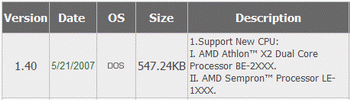
As of November 2007, AMD has removed the letters from the model names and X2/X3/X4 monikers for depicting the number of cores of the processor, leaving just a four digit model number with the first character being the sole identification of the processor family,[26] while Sempron remained using the LE prefix, as follows:
| Processor series | Indicator |
|---|---|
| Phenom quad-core (Agena) | 9 |
| Phenom triple-core (Toliman) | 8 |
| Athlon dual-core (Kuma) | 7 |
| Athlon single-core (Lima) | 1 |
| Sempron LE single-core (Sparta) | 1 |
Live demonstrations
On November 30, 2006, AMD live demonstrated the native quad core chip known as "Barcelona" for the first time in public,[28] while running Windows Server 2003 64-bit Edition. AMD claims 70% scaling of performance in real world loads, and better performance than Intel Xeon 5355 processor codenamed Clovertown.[29] More details regarding this first revision of the next generation AMD microprocessor architecture have surfaced on the web including their clock speeds.[30][31]
On January 24, 2007, AMD Executive Vice President Randy Allen claimed that in live tests, in regard to a wide variety of workloads, "Barcelona" was able to demonstrate 40% performance advantage over the comparable Intel Xeon codenamed Clovertown dual-processor (2P) quad-core processors.[32] The expected performance of floating point per core would be approximately 1.8 times that of the K8 family, at the same clock speed.[33]
On May 10, 2007, AMD held a private event demonstrating the upcoming processors codenamed Agena FX and chipsets, with one demonstrated system being AMD Quad FX platform with one Radeon HD 2900 XT graphics card on the upcoming RD790 chipset, the system was also demonstrated real-time converting a 720p video clip into another undisclosed format while all 8 cores were maxed at 100% by other tasks.[34]
Sister microarchitecture
Also due in a similar time frame will be a sister microarchitecture, which will focus on lower power consumption chips in mobile platforms as well as small form factor features. This microarchitecture will contain specialized features such as mobile optimized crossbar switch and memory controller and other on-die components; link power management for HyperTransport 3.0; and others. At that time, AMD simply dubbed it "New Mobile Core", without giving a specific codename.
On the December 2006 analyst day, Executive vice president Marty Seyer announced the new mobile core codenamed Griffin launched in 2008 with inherited power optimizations technologies from the K10 microarchitecture, but based on a K8 design
Iterations of the release
In late 2007 to second quarter of 2008, there will be a modification to the core to be fabricated at 45 nm process node,[35] with enhancements such as FB-DIMM support, Direct Connect Architecture 2.0, enhanced Reliability, Availability and Serviceability (RAS), and probably more for the processor die. The platform will also add support for I/O Virtualization, PCI Express 2.0, 10 Gigabit NIC, larger caches, and more.
However, reports have suggested that FB-DIMM support had been dropped from future roadmaps of the majority of AMD products since popularity is low.[36][37] Also, FB-DIMM's future as an industry standard had been called into question.
An article published by The Inquirer corroborates the earlier reports of the timeline (as cited in this article). According to the report, there will be three iterations of the server processor core: one named Barcelona, due in Q2 of 2007, with new CPU core components as well as the microarchitecture, but built on the old HyperTransport 2.0 infrastructure; the second is Budapest for single socket systems using socket AM2+ or socket AM3, with HyperTransport 3.0; and the third, codenamed Shanghai is an update of the server chip, based on 45 nm process,[38] probably also with HyperTransport 3.0 and DDR3 implementation, due in Q1-Q2 2008.[39]
AMD, on September 17, 2007, announced [40] that a three core (triple-core) processor will also be released under the Phenom brand lineup, codenamed Toliman. AMD official replied in an interview that this product is benefitted from ATI technologies to add fuses to the quad-core processor and shutting down one of the four cores [41] to become a triple-core processor, which the technique has been popular for making one or more mainstream GPU cores from a single high-end GPU core by blowing out parts of the circuit to save R&D costs while targeting more markets some time ago. The triple-core processor still see the same specifications for quad-core variants, the naming of the processor lineup, according to the AMD branding scheme, will be named as Phenom triple-core 8000 series, the processor line will be focused on what AMD called the fourth market segment or the "High-end Mainstream" segment beside Value, Mainstream and Performance segments in an interview with BetaNews, which the targeted customers of the processors are "those who are willing to pay more for more performance but not required for too much processing power as required by gamers and system builders",[42][43] while there are single core (Sempron) variants for low-end market, and dual-core (Athlon) variants for mid-range market, and quad-core (Phenom quad-core 9000 series and Phenom FX) variants should be seen in the high-end market at the same time frame.
Further in 2008, AMD will introduce Deneb FX for the replacement for the AMD Quad FX platform, as well as Deneb for the mainstream. Propos and Regor will also replace Kuma and Rana in the lower market segments. Socket AM2+ being named in the late 2006 might actually have been the original AM3 socket, but as naming conventions changed, so that the next generation of consumer desktop socket capable of DDR3 will be socket AM3.[44]
Features
Fabrication technology
AMD has introduced the microprocessors manufactured at 65 nm feature width using Silicon-on-insulator (SOI) technology, since the release of K10 coincides with the volume ramp of this manufacturing process.[45] The servers will be produced for Socket F(1207) or later 1207-pin socket infrastructure, the only server socket on AMD's near-term roadmap; the desktop parts will come on Socket AM2 or Socket AM2+.
AMD announced during the Technology Analyst Day [46] that the use of Continuous Transistor Improvement (CTI) and Shared Transistor Technology (STT) would finally lead to the implementation of Silicon-Germanium-On-Insulator (SGoI) on 65 nm process CPUs.[47]
Supported DRAM standards
The K8 family was known to be particularly sensitive to memory latency since its design gains performance by minimizing this through the use of an on-die memory controller (integrated into the CPU); increased latency in the external modules negates the usefulness of the feature. DDR2 RAM introduces some additional latency over traditional DDR RAM since the DRAM is internally driven by a clock at one quarter of the external data frequency, as opposed to one half that of DDR. However, since the command clock rate in DDR2 is doubled relative to DDR and other latency-reducing features (e.g. additive latency) have been introduced, common comparisons based on CAS latency alone are not sufficient. For example, Socket AM2 processors are known to demonstrate similar performance using DDR2 SDRAM as Socket 939 processors that utilize DDR-400 SDRAM. K10 processors support DDR2 SDRAM rated up to DDR2-1066 (1066 MHz).[48]
Higher computational throughput
It was also reported by several sources (such as AnandTech, The Inquirer and Geek.com) that the microprocessors implementing the microarchitecture will feature a doubling in the width of SSE execution units in the cores. With the help of major improvements in the memory subsystem (such as load re-ordering and improved prefetch mechanisms) as well as the doubled instruction fetch and load, it is expected to increase the suitability of the processor to scientific and high-performance computing tasks and potentially improve its competitiveness with Intel's Xeon, Core 2, Itanium 2 and other contemporary microprocessors.
Many of the improvements in computational throughput of each core are listed below.
Microarchitecture characteristics
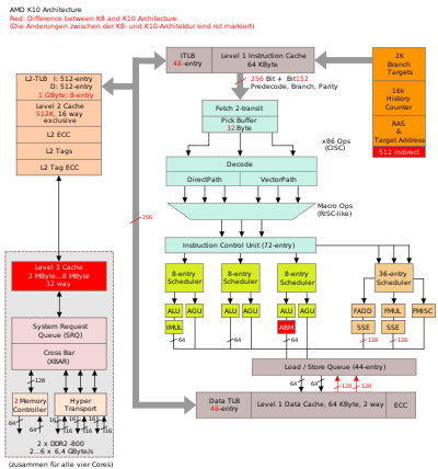

Characteristics of the microarchitecture include the following:[49]
- Form factors
- Socket AM2+ with DDR2 for the 65 nm Phenom and Athlon 7000 Series
- Socket AM3 with either DDR2 or DDR3 for the 45 nm Phenom II Series. Note that, while all K10 Phenom Processors are backwards compatible with Socket AM2+ and Socket AM2, some 45 nm Phenom II Processors are only available for Socket AM2+.
- Socket F with DDR2, DDR3 with Shanghai and later
- Instruction set additions and extensions
- New bit-manipulation instructions ABM: Leading Zero Count (LZCNT) and Population Count (POPCNT)
- New SSE instructions named as SSE4a: combined mask-shift instructions (EXTRQ/INSERTQ) and scalar streaming store instructions (MOVNTSD/MOVNTSS). These instructions are not found in Intel's SSE4
- Support for unaligned SSE load-operation instructions (which formerly required 16-byte alignment)[50]
- Execution pipeline enhancements
- 128-bit wide SSE units
- Wider L1 data cache interface allowing for two 128-bit loads per cycle (as opposed to two 64-bit loads per cycle with K8)
- Lower integer divide latency
- 512-entry indirect branch predictor and a larger return stack (size doubled from K8) and branch target buffer
- Side-Band Stack Optimizer, dedicated to perform increment/decrement of register stack pointer
- Fastpathed CALL and RET-Imm instructions (formerly microcoded) as well as MOVs from SIMD registers to general purpose registers
- Integration of new technologies onto CPU die:
- Four processor cores (Quad-core)
- Split power planes for CPU core and memory controller/northbridge for more effective power management, first dubbed Dynamic Independent Core Engagement or D. I. C. E. by AMD and now known as Enhanced PowerNow! (also dubbed Independent Dynamic Core Technology), allowing the cores and northbridge (integrated memory controller) to scale power consumption up or down independently.[51]
- Shutting down portions of the circuits in core when not in load, named "CoolCore" Technology.
- Improvements in the memory subsystem:
- Improvements in access latency:
- Support for re-ordering loads ahead of other loads and stores
- More aggressive instruction prefetching, 32 bytes instruction prefetch as opposed to 16 bytes in K8
- DRAM prefetcher for buffering reads
- Buffered burst writeback to RAM in order to reduce contention
- Changes in memory hierarchy:
- Prefetch directly into L1 cache as opposed to L2 cache with K8 family
- 32-way set associative L3 victim cache sized at least 2 MB, shared between processing cores on a single die (each with 512 K of independent exclusive L2 cache), with a sharing-aware replacement policy.
- Extensible L3 cache design, with 6 MB planned for 45 nm process node, with the chips codenamed Shanghai.
- Changes in address space management:
- Two 64-bit independent memory controllers, each with its own physical address space; this provides an opportunity to better utilize the available bandwidth in case of random memory accesses occurring in heavily multi-threaded environments. This approach is in contrast to the previous "interleaved" design, where the two 64-bit data channels were bounded to a single common address space.
- Larger Tagged Lookaside Buffers; support for 1 GB page entries and a new 128-entry 2 MB page TLB
- 48-bit memory addressing to allow for 256 TB memory subsystems[52]
- Memory mirroring (alternatively mapped DIMM addressing),[53] data poisoning support and Enhanced RAS
- AMD-V Nested Paging for improved MMU virtualization, claimed to have decreasing world switch time by 25%.
- Improvements in access latency:
- Improvements in system interconnect:
- HyperTransport retry support
- Support for HyperTransport 3.0, with HyperTransport Link unganging which creates 8 point-to-point links per socket.
- Platform-level enhancements with additional functionality:
- Five p-states allowing for automatic clock rate modulation
- Increased clock gating
- Official support for coprocessors via HTX slots and vacant CPU sockets through HyperTransport: Torrenza initiative.
Phenom Models
Agena (65 nm SOI)
- Four AMD K10 cores
- L1 cache: 64 KB instruction and 64 KB data[54] (data + instructions) per core
- L2 cache: 512 KB per core, full-speed
- L3 cache: 2 MB shared between all cores
- Memory controller: dual channel DDR2-1066 MHz with unganging option
- MMX, Extended 3DNow!, SSE, SSE2, SSE3, SSE4a, AMD64, Cool'n'Quiet, NX bit, AMD-V
- Socket AM2+, HyperTransport with 1600 to 2000 MHz
- Power consumption (TDP): 65, 95, 125 and 140 Watt
- First release
- November 19, 2007 (B2 Stepping)
- March 27, 2008 (B3 Stepping)
- Clock rate: 1800 to 2600 MHz
- Models: Phenom X4 9100e - 9950
Toliman (65 nm SOI)
- Three AMD K10 cores
- L1 cache: 64 KB instruction and 64 KB data cache per core
- L2 cache: 512 KB per core, full-speed
- L3 cache: 2 MB shared between all cores
- Memory controller: dual channel DDR2-1066 MHz with unganging option
- MMX, Extended 3DNow!, SSE, SSE2, SSE3, SSE4a, AMD64, Cool'n'Quiet, NX bit, AMD-V
- Socket AM2+, HyperTransport with 1600 to 1800 MHz
- Power consumption (TDP): 65 and 95 Watt
- First release
- March 27, 2008 (B2 Stepping)
- April 23, 2008 (B3 Stepping)
- Clock rate: 2100 to 2500 MHz
- Models: Phenom X3 8250e - 8850
Phenom II Models
Thuban (45 nm SOI with Immersion Lithography)
- Six AMD K10 cores
- L1 cache: 64 KB instructions and 64 KB data per core
- L2 cache: 512 KB per core, full-speed
- L3 cache: 6 MB shared between all cores.
- Memory controller: dual channel DDR2-1066 MHz (AM2+), dual channel DDR3-1333 (AM3) with unganging option
- MMX, Extended 3DNow!, SSE, SSE2, SSE3, SSE4a, AMD64, Cool'n'Quiet, NX bit, AMD-V
- Socket AM2+, Socket AM3, HyperTransport with 1800 to 2000 MHz
- Power consumption (TDP): 95 or 125 Watt
- First release
- 27 April 2010 (E0 Stepping)
- Clock rate: 2.6 - 3.3 GHz; up to 3.7 GHz with Turbo Core
- Models: Phenom II X6 1035T, 1045T, 1055T, 1065T, 1075T, 1090T and 1100T
- Models: Phenom II X4 840T, 960T, 970 (Thuban-based Zosma core, OEM Only, 970 has unlocked multiplier but w/o Turbo Core)
Deneb (45 nm SOI with Immersion Lithography)
- Four AMD K10 cores
- L1 cache: 64 KB instructions and 64 KB data per core
- L2 cache: 512 KB per core, full-speed
- L3 cache: 6 MB shared between all cores. The 800 series have 2 MB of its L3 Cache disabled due to defects.
- Memory controller: dual channel DDR2-1066 MHz (AM2+), dual channel DDR3-1333 (AM3) with unganging option
- MMX, Extended 3DNow!, SSE, SSE2, SSE3, SSE4a, AMD64, Cool'n'Quiet, NX bit, AMD-V
- Socket AM2+, Socket AM3, HyperTransport with 1800 to 2000 MHz
- Power consumption (TDP): 65, 95, 125 and 140 Watt
- First release
- 8 January 2009 (C2 Stepping)
- Clock rate: 2500 to 3700 MHz
- Models: Phenom II X4 805 - 980
Heka (45 nm SOI with Immersion Lithography)
- Three AMD K10 cores using chip harvesting technique, with one core disabled
- L1 cache: 64 KB instructions and 64 KB data per core
- L2 cache: 512 KB per core, full-speed
- L3 cache: 6 MB shared between all cores
- Memory controller: dual channel DDR2-1066 MHz (AM2+), dual channel DDR3-1333 (AM3) with unganging option
- MMX, Extended 3DNow!, SSE, SSE2, SSE3, SSE4a, AMD64, Cool'n'Quiet, NX bit, AMD-V
- Socket AM3, HyperTransport with 2000 MHz
- Power consumption (TDP): 65 and 95 Watt
- First release
- 9 February 2009 (C2 Stepping)
- Clock rate: 2500 to 3000 MHz
- Models: Phenom II X3 705e - 740
Callisto (45 nm SOI with Immersion Lithography)
- Two AMD K10 cores using chip harvesting technique, with two cores disabled
- L1 cache: 64 KB instructions and 64 KB data per core
- L2 cache: 512 KB per core, full-speed
- L3 cache: 6 MB shared between all cores
- Memory controller: dual channel DDR2-1066 MHz (AM2+), dual channel DDR3-1333 (AM3) with unganging option
- MMX, Extended 3DNow!, SSE, SSE2, SSE3, SSE4a, AMD64, Cool'n'Quiet, NX bit, AMD-V
- Socket AM3, HyperTransport with 2000 MHz
- Power consumption (TDP): 80 Watt
- First release
- 1 June 2009 (C2 Stepping)
- Clock rate: 3000 to 3500 MHz
- Models: Phenom II X2 545 - 570
Athlon II Models
Regor (45 nm SOI with Immersion Lithography)
- Two AMD K10 cores
- L1 cache: 64 KB instructions and 64 KB data per core
- L2 cache: 1024 KB per core, full-speed
- Memory controller: dual channel DDR2-1066 MHz (AM2+), dual channel DDR3-1333 (AM3) with unganging option
- MMX, Extended 3DNow!, SSE, SSE2, SSE3, SSE4a, AMD64, Cool'n'Quiet, NX bit, AMD-V
- Socket AM3, HyperTransport with 2000 MHz
- Power consumption (TDP): 65 Watt
- First release
- June 2009 (C2 Stepping)
- Clock rate: 2800 - 3600 MHz
- Models: Athlon II X2 240 - 280
Propus (45 nm SOI with Immersion Lithography)
- Four AMD K10 cores
- L1 cache: 64 KB instructions and 64 KB data per core
- L2 cache: 512 KB per core, full-speed
- Memory controller: dual channel DDR2-1066 MHz (AM2+), dual channel DDR3-1333 (AM3) with unganging option
- MMX, Extended 3DNow!, SSE, SSE2, SSE3, SSE4a, AMD64, Cool'n'Quiet, NX bit, AMD-V
- Socket AM3, HyperTransport with 2000 MHz
- Power consumption (TDP): 45 Watt or 95 Watt
- First release
- September 2009 (C2 Stepping)
- Clock rate: 2200 - 3100 MHz
- Models: Athlon II X4 600e - 645
Successor
AMD discontinued further development of K10 based CPUs after Thuban, choosing to focus on Fusion products for mainstream desktops and laptops and Bulldozer based products for the performance market. However, within the Fusion product family, APUs such as the first generation A4, A6 and A8-series chips (Llano APUs) continued to use K10-derived CPU cores in conjunction with a Radeon graphics core. K10 and its derivatives were phased out of production by the introduction of Trinity-based APUs in 2012, which replaced the K10 cores in the APU with Bulldozer-derived cores.
Family 11h and 12h derivatives
Turion X2 Ultra Family 11h
The Family 11h microarchitecture was a mixture of both K8 and K10 designs with lower power consumption for laptop that was marketed as Turion X2 Ultra and was later replaced by completely K10-based designs.[1]
Fusion Family 12h
The Family 12h microarchitecture is a derivative of the K10 design:[57][58]
- Both CPU and GPU were re-used to avoid complexity and risk
- Distinct Software and Physical integration makes Fusion (APU) microarchitectures different
- Power-saving improvements including clock gating
- Improvements to hardware pre-fetcher
- Redesigned memory controller
- 1MB L2 cache per core
- No L3 cache
- Two new buses for on-die GPU to access memory (called Onion and Garlic interfaces)
- AMD Fusion Compute Link (Onion) - interfaces to CPU cache and coherent system memory (see cache coherence)
- Radeon Memory Bus (Garlic) - dedicated non-coherent interface connected directly to memory
Media discussions
Note: These media discussions are listed in ascending date of publication.
- "AMD CTO speaks about future AMD technologies". AnandTech. 2005-10-14.
- "AMD outlines Future Goals (mostly non-specific at this time)". TechReport. 2005-10-17.
- "AMD eyes Z-RAM for dense caches". CNet News.com. 2006-01-20.
- "AMD licenses Z-RAM". SlashDot. 2006-01-21.
- "AMD's K8L to double FPU units in 2007". Geek.com. 2006-02-24.
- "Rev G. and H. AMD64 chips Preliminary information". The Inquirer. 2006-03-03.
- "Interview with Henri Richard (Part 2)". DigiTimes. 2006-03-14.
- "AMD demonstrates Hardware Coprocessor Offload". LinuxElectrons. 2006-03-20.
- "Implementation of FPGA through coherent HTT". The Inquirer. 2006-03-26.
- "AMD's K8L 65 nm core due H1 07". Reg Hardware. 2006-04-04.
- "An AMD Update: Fab 36 Begins Shipments, Planning for 65 nm and AM2 Performance". AnandTech. 2006-04-04.
- "Fab36 substantially converted to 65 nm by mid-2007". AnandTech. 2006-04-04.
- "AMD shows off details of K8L". The Inquirer. 2006-05-16.
- "AMD's K8L and 4x4 Preview". RealWorldtech. 2006-06-02.
- "AMD K8L and 4X4 Technologies". ArsTechnica. 2006-06-02.
- "AMD Quad-Core K8L & 4x4 Details". Pure OverClock. 2006-06-03. Archived from the original on February 9, 2012.
- "Socket AM2 Forward Compatible With AM3 CPUs". DailyTech. 2006-07-06.
- "K8L on schedule, due for release as early as Q1 07". The Inquirer. 2006-07-11. Archived from the original on September 6, 2007.
- "GNU binutils support for the new K10 instructions". SourceWare.org. 2006-07-13.
- "AMD Executives Confirm K8L to Arrive in Mid-2007". X-bit labs. 2006-07-21.
- "AMD To Demo K8L By Year End". moneycontrol.com. 2006-07-23. Archived from the original on August 18, 2007.
- "AMD intros new Opterons and promises 68 W quad-core CPUs". tgdaily.com. 2006-08-15.
- "Next-Generation AMD Opteron Paves The Way For Quad-Core". crn.com. 2006-08-15.
- "AMD's Next Generation Microarchitecture Preview: from K8 to K8L". X-bit labs. 2006-08-21.
- "AMD quad cores: the whole story unfolded". The Inquirer. 2006-09-16. Archived from the original on May 19, 2007.
- "AMD reinvents the x86". InfoWorld. 2007-02-07. Archived from the original on December 7, 2008.
- "Inside Barcelona: AMD's Next Generation". RealWorldTech. 2007-05-16.
See also
- AMD K9
- Phenom (processor)
- Phenom II
- List of AMD Phenom microprocessors
- List of AMD Athlon X2 microprocessors
References
- 1 2 "List of AMD CPU microarchitectures - LeonStudio". LeonStudio - CodeFun. 3 August 2014. Retrieved 12 September 2015.
- ↑ AMD's K10 is delayed or dead, The Inquirer
- ↑ Hesseldahl, Arik (2000-07-06). "Why Cool Chip Code Names Die". forbes.com. Forbes.com Inc. Retrieved 2007-07-14.
- ↑ The Inquirer report Archived September 6, 2007, at the Wayback Machine.
- 1 2 Valich, Theo. "AMD explains K8L misnomer". The Inquirer. Archived from the original on February 10, 2007. Retrieved 2007-03-16.
- ↑ Official Announcement of "AMD Next Generation Processor Technology"
- ↑ Video interview of Giuseppe Amato (AMD's Technical Director, Sales and Marketing EMEA) in February 2007
- ↑ Microprocessor Forum 2003 presentation slide
- ↑ Hall, Chris. "Re-defining microprocessors: Q&A with AMD's Henri Richard". DigiTimes.com. Archived from the original on March 13, 2006. Retrieved 2007-03-18.
- ↑ AMD's vision for next few years - an interview with Henri Richard
- ↑ "Next-Generation AMD Opteron Paves The Way For Quad-Core". crn.com. 2006-08-15.
- ↑ "AMD to Ship Industry's First Native x86 Quad-Core Processors In August". amd.com. 2007-06-29.
- ↑ "AMD to launch two Barcelona-based processors in September". tgdaily.com. 2007-08-13.
- ↑ dailytech.com: Understanding AMD's TLB Processor Bug, December 5, 2007
- ↑ xbitlabs.com: ... TLB Bug – in the Past, March 26, 2008
- ↑ "AMD Quad-Core Altair upcoming in 2007 Q3". HKEPC. 2006-10-03.
- ↑ "AMD to enter K10 era in 2H 2007". HKEPC. 2006-10-04.
- ↑ "2006 Analyst Day Slides".
- ↑ The Inquirer report Archived September 12, 2007, at the Wayback Machine.
- ↑ FudZilla report
- ↑ FudZilla report
- ↑ Fudzilla report, retrieved August 1, 2007 Archived October 16, 2007, at the Wayback Machine.
- ↑ "How to decipher AMD's new CPU naming code". Gadget Lab. 2007-06-04.
- 1 2 DailyTech report
- ↑ XTReview image: AsRock BIOS 1.40 support Athlon X2 BE-xxxx and Sempron LE-xxxx processors
- ↑ "AMD Revised Desktop Model Number Structure". VR-Zone. 2007-10-09. Archived from the original on October 11, 2007.
- ↑ VR-Zone report, retrieved October 9, 2007 Archived October 11, 2007, at the Wayback Machine.
- ↑ "AMD Demonstrates Its Quad Core Server Chips". CNET.com. 2006-11-30.
- ↑ "AMD Demonstrates Barcelona; The First True, Native Quad Core Opteron". legitreviews.com. 2006-11-30.
- ↑ "Quick Look at AMD Quad Core Barcelona". arstechnica.com. 6 December 2006.
- ↑ The Inquirer article Archived May 16, 2007, at the Wayback Machine.
- ↑ "AMD Expects Quad Core Barcelona to Outperform Clovertown by 40%". dailytech.com. 2007-01-25.
- ↑ "Go to 'Barcelona' over 'Cloverton'". CNET.com. 2007-01-23.
- ↑ TGDaily report
- ↑ "AMD Outlines Quad Core Computing". www.pcpro.co.uk. 2006-09-19.
- ↑ "Intel Pulls Back from FB-DIMM". inquirer.net. 2006-09-07.
- ↑ "No Shocker Here". legitreviews.com. 2006-09-15.
- ↑ DailyTech report
- ↑ "AMD Quad Cores: The Whole Story Unfolded". inquirer.net. 2006-09-16. Archived from the original on May 19, 2007.
- ↑ AMD announcement, retrieved September 17, 2007
- ↑ ComputerWorld report Archived October 12, 2007, at the Wayback Machine., retrieved October 9, 2007
- ↑ BetaNews report, retrieved September 17, 2007
- ↑ BetaNews interview, retrieved September 17, 2007
- ↑ "AMD: 45nm, DDR3, and AM3 in 2008". dailytech.com. 2007-05-02.
- ↑ "An AMD Update: Fab 36 Begins Shipments, Planning for 65 nm process and AM2 Performance". AnandTech. 2006-04-04.
- ↑ 2006 AMD Analyst Day 2006 page Archived May 17, 2009, at the Wayback Machine.
- ↑ Ostrander, Daryl. "2006 Technology Analyst Day Slides" (PDF). Advanced Micro Devices. Archived from the original (PDF) on January 13, 2007. Retrieved 2007-03-19.
- ↑ "AMD's next-generation Star supports DDR2-1066 & SSE4a". HKEPC Hardware. Retrieved 2007-03-19.
- ↑ Shimpi, Anand Lal. "Barcelona Architecture: AMD on the Counterattack". AnandTech. Archived from the original on 19 March 2007. Retrieved 2007-03-18.
- ↑ Case, Loyd. "AMD Unveils Barcelona Quad-Core Details". Ziff Davis. Retrieved 2007-03-18.
- ↑ "AMD Next Generation Processor Technology Slides". HardOCP. 2006-08-22.
- ↑ "BIOS and Kernel Developer's Guide (BKDG) For AMD Family 10h Processors" (PDF). p. 24. Archived from the original (PDF) on June 9, 2011. Retrieved 2010-05-29.
Physical address space increased to 48 bits.
- ↑ "BIOS and Kernel Developer's Guide (BKDG) for AMD Family 15h Models 10h-1Fh Processors" (PDF). support.amd.com. Advanced Micro Devices. June 4, 2013. p. 340. Retrieved January 25, 2015.
- ↑ In this article, the conventional prefixes for computer memory denote base-2 values whereby “kilobyte” (KB) = 210 bytes.
- ↑ Athlon II: Viele neue Exemplare der neuen Einsteiger-Prozessoren von AMD
- ↑ In arrivo nuovi processori Athlon II da AMD Archived July 10, 2011, at the Wayback Machine.
- ↑ David Kanter (27 June 2011). "AMD Fusion Architecture and Llano". Real World Tech. Retrieved 12 September 2015.
- ↑ Pierre Boudier; Graham Sellers (June 2011). "Memory System on Fusion APUs - The Benefits of Zero Copy". AMD Fusion Developer Summit.
External links
- AMD Official Website
- AMD Quad-core processors introduction
- DarkVision Hardware: AMD talks about K9, K10 future innovations
- Next-Generation AMD Opteron Processors Introduced with Record OEM Design Wins and Native Quad-Core Upgrade Path (Official AMD press release on 15 August 2006)
- PC Watch report about K10 based on AMD Technology Analyst Day 2004 and 2005 (Japanese)
- PC Watch report about K10 based on Slides presented in Microprocessor Forum 2003 (Japanese)
- "Slides of AMD 2006 Technology Analyst Day: Official Introduction of K10 Microarchitecture" (PDF). Archived from the original on 2009-03-26. (2.17 MB)
- Software Optimization Guide for AMD Family 10h and 12h Processors
- TechReport: AMD outlines Future Goals
- TweakTown Discussions (2003)
- X-bit labs: AMD K10 Micro-Architecture